 |
Home > Offers to Sell > Electronics & Electrical > Passive Components > Other PCB & PCBA
| Contact: | alisa.lu |
|---|---|
| Company: | Shenzhen Fast PCB Technology Co.,Ltd. |
| 广东省深圳市宝安区西乡街道草围社区第二工业区 | |
| shenzhen 518126 | |
| China | |
| Phone: | 18870167235 |
| E-Mail: | |
| Date/Time: | 7/3/22 7:43 GMT |
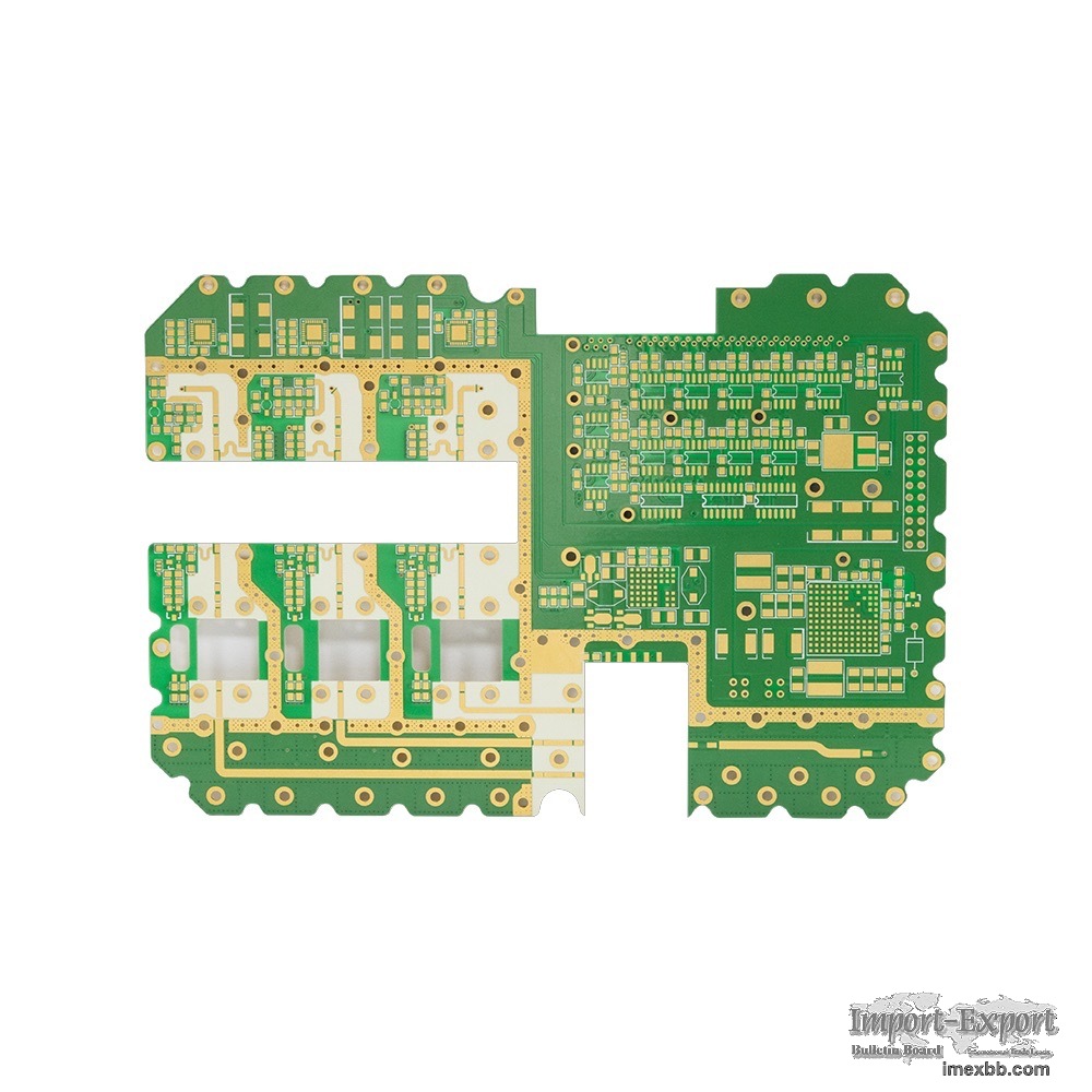
rigid-flex printed circuit board
Layer Count & Material
Layers 1-8Layers Maximum Panel Size 19.6*31.0 inch
Maximum Single Unit Size 9inch*14inch (limitation is
9inch*23inch) Minimum Panel Size 9.0*12.0 inch
Board Size Tolerance ±0.1mm Maximum Finished Board Thickness 0.80mm
Minimum Finished Board Thickness 0.05mm
Trace/Line
Minimum Line Width for Inner Layers 3mil Minimum Line Spacing for Outer
Layers 3.5mil
Minimum Line Width for Outer Layers 3mil The Copper Thickness for Inner
Layers ≤2OZ
Minimum Line Spacing for Inner 3mil The Copper Thickness for Outer Layers
≤3OZ
Drilling
Minimum Hole Diameter 0.15mm Minimum Distance from Hole to Board Outline
8mil
Maximum Hole Diameter 6.4mm Minimum Size for Hole Ring 4mil
(Partially 3.2mil)
Hole Diameter Tolerance ±2mil The Minimum BGA Bonding Pad Design ≥8mil
(7mil is the Limitation)
The Distance from Hole to Hole 10mil The Minimum SMT Design ≥7mil
Solder Mask
SM Bridge Width ≥4mil Minimum Width of Legend 4mil
Minimum Size of SM Window 3mil(Partially 2.5mil) Minimum Hight of
Legend 23mil
The Minimum Distance from SM Window to Other Outline 3mil
Surface Finished
HASL、ENIG、ENEPIG、Soft bonding gold(Soft Gold Plating)、Hard Gold Plating、
Immersion Silver、OSP、Immersion Tin、ENIG+OSP、ENIG+G/F
Impedance
Whether it is capable of impedance testing Yes, it capable, it have
Minimum Order: 1 pieces
SOURCE: Import-Export Bulletin Board (https://www.imexbb.com/)
Similar Products:Not exactly what you are looking for? Post an Offer to Buy!
![]()
© 1996-2010 IMEXBB.com. All rights reserved.
|
|
|


