 |
 |
Home > Offers to Sell > Electronics & Electrical > Switches > Key & Rotary Switches
| Contact: | speedapcb |
|---|---|
| Company: | Hunan Speeda Technology Co.,Ltd. |
| 4F,wangdefu Building,Wanjiali Road,Furong District,Changsha,Hunan | |
| Changsha 427000 | |
| China | |
| Phone: | 86 15387574935 |
| E-Mail: | |
| Date/Time: | 11/11/20 7:42 GMT |
4 Layer PCB
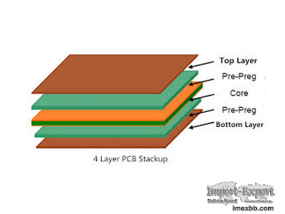
In general, in a 4 layer pcb prototype , both the top and bottom layers belong
to the signal layer, while another two inner layers are GND and VCC. If the
first inner layer has several GND planes, the blank areas of which should be
filled with copper. It could also have some routings, but do remember these
routings are not allowed to cross the copper area. Same to the second layer
with several powers. Usually, layers of a 4 layer PCB are connected by plated
through holes, buried holes, and blind holes while layers of a 2 layer PCB are
only connected by plated through holes. Besides, if possible, VCC and GND
should not serve as signal layers.
There are insulation materials between the two layers. After every layer is
printed with circuits, we could use lamination to make circuits overlap and use
drills to make via holes to connect circuits. Since a 4 layer, PCB has routings
in several layers, it is a good choice if you want to design elaborate products
in small sizes, like mobile phone circuit boards, mini-projectors, and
recorders. In addition, multi-layers provide broader space for design, control
differential characteristic and single-ended impedance, and better the output
of signal frequency.
Right now, our electronic devices continue to pursue higher speed, larger
capacity, and smaller size. Therefore, 4 layer PCB is a product that emerges as
the times require. Later plated through holes, buried holes and blind holes
come into being to meet people’s needs to produce circuit boards with greater
density, precision. Now that computer and aerospace industries are in great
need of high-speed circuits, they are asking for components with higher
packaging density. Besides, discrete components are getting smaller,
microelectronics is facing rapid development, and electronic devices are
turning into smaller and lighter ones. With such background, the single-sided
or double-sided printed boards are not capable to increase the packaging
density because they have restrictions brought up by limited space.
SPEEDA Technology is an electronic technology company formed by a team with an
average of 10+ years of electronic industry experience. As one of the best
circuit board suppliers, the company is mainly engaged in the design, R&D
(research and development), manufacturing, and sales of various printed circuit
boards. The products are widely used in communication equipment, computer and
network equipment, consumer electronics, automotive electronics, industrial
control, new energy, rail transit, and other industries. We provide customers
with a "one-stop" service, that is, an integrated service system consisting of
printed circuit board design optimization, small-batch sample production, batch
production, and after-sale services. Adhere to quality first, service first, to
improve customer satisfaction as the goal continuously.
SPEEDA, Your Best Business Partner.
SOURCE: Import-Export Bulletin Board (https://www.imexbb.com/)
Similar Products:Not exactly what you are looking for? Post an Offer to Buy!
![]()
© 1996-2010 IMEXBB.com. All rights reserved.
|
|
|


